6-Layer PCB

6-Layer PCB

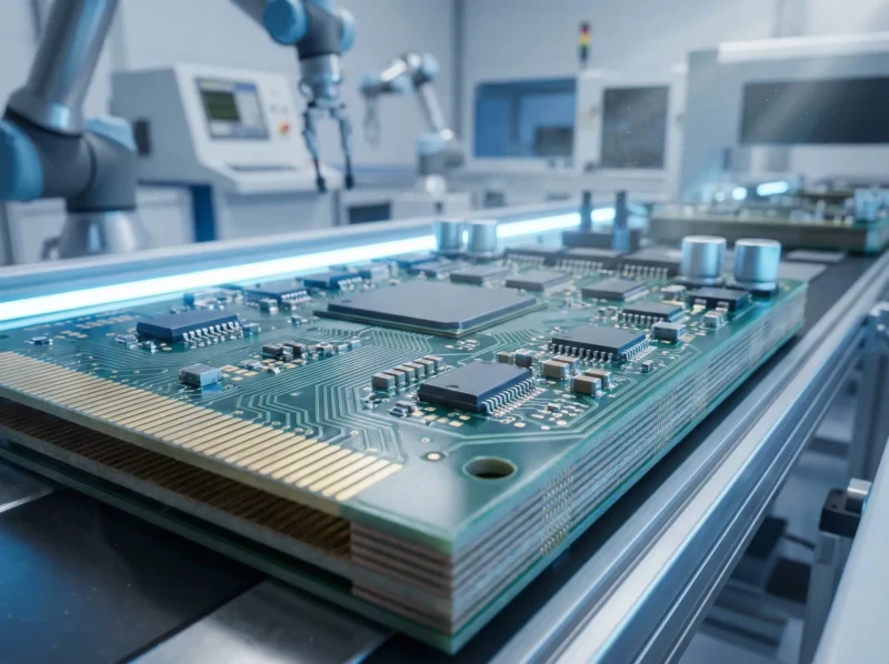
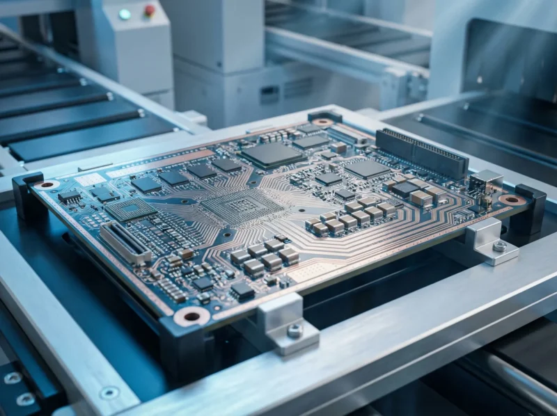
Complex 6-layer designs for demanding signal integrity requirements. Supports high-Tg materials and controlled impedance for server and communication equipment.

Layers 6
Material FR-4 (TG135-TG250)
Thickness 0.6-4.0mm
Copper Weight 0.5-6oz
Max Size 650×2000mm
Min Trace/ Space 3/3 mil
Min Drill 0.15mm
Impedance Control ±10%
Blind/ Buried Via Yes
Surface Finish HASL, Lead-free HASL, ENIG, OSP, Immers ion Silver,Immers ion Tin
Solder Mask green, black, white, red, blue
Silkscreen white, black

Request a Quote

Enter the quantity you need and add to your quote list for pricing inquiries.

Description

Technical Specifications

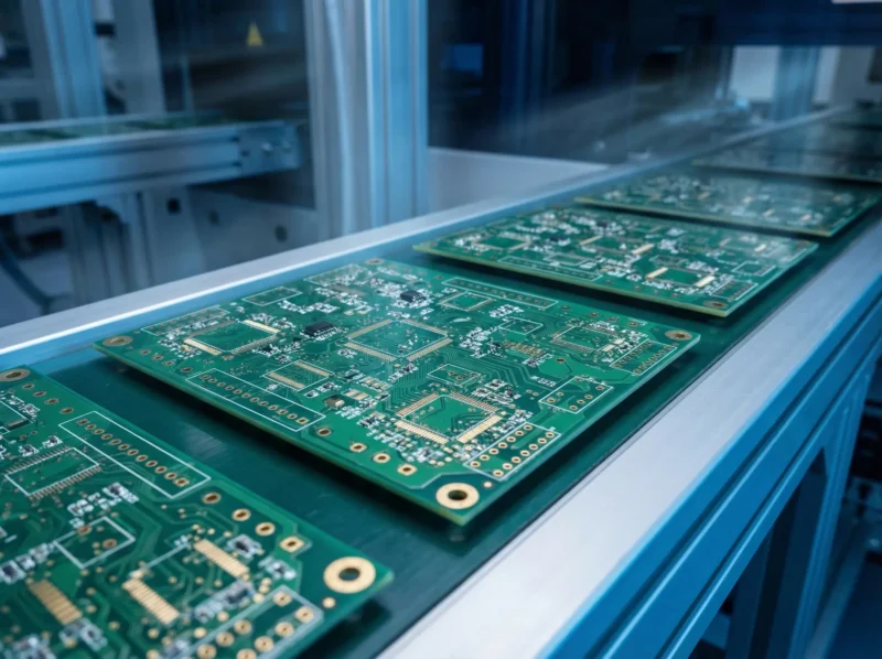
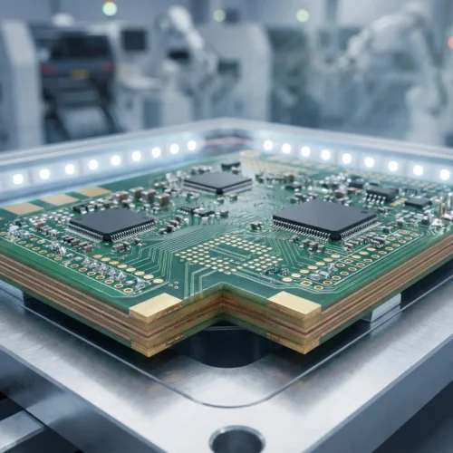
6-layer PCB construction addresses the design space between basic multilayer boards and high-density interconnect structures, offering two additional routing or plane layers that significantly expand electrical design flexibility. XinAn PCB fabricates 6-layer boards on FR-4 with Tg ratings from 135°C to 250°C, achieving minimum trace/space of 3mil/3mil and minimum via diameter of 0.15mm mechanical or 0.1mm laser. The 6-layer stackup is the preferred choice for telecommunications equipment, server motherboards, automotive ADAS modules, and networking switches where signal integrity, power distribution, and EMC performance demand more than four layers can provide. Our 6-layer production maintains ±7% impedance tolerance and ±2mil interlayer registration.
Stackup Architecture and Signal Integrity

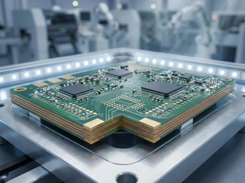
The standard 6-layer stackup follows a signal/ground/signal/signal/power/signal arrangement, though we frequently produce ground/signal/ground/power/signal/ground configurations for designs requiring superior EMI performance. The additional two layers allow dedicated ground and power planes while preserving two internal routing layers—a critical advantage for BGA fanout on devices with 0.8mm or 0.65mm ball pitch. With two continuous reference planes, return current paths are well-defined and shorter, reducing loop inductance and improving signal integrity for DDR4 memory interfaces operating at 2400-3200MT/s. We use broadside-coupled differential pairs on internal layers for LVDS, USB 3.0, and PCIe Gen3 signals, achieving 85-100Ω differential impedance with 5-7mil trace widths and 5-8mil spacing depending on dielectric thickness.

Power Distribution and Thermal Management

The 6-layer stackup’s dedicated power and ground planes create a low-impedance power distribution network (PDN) with distributed capacitance between the plane pair. For a standard 47mil core between power and ground planes, the inter-plane capacitance is approximately 90pF/cm², providing inherent high-frequency decoupling above 500MHz. Designers can further optimize PDN impedance by specifying thinner dielectric between the plane pair—down to 4mil with appropriate laminate selection—increasing inter-plane capacitance to over 500pF/cm². Thermally, the additional copper layers improve heat spreading from power components. A 6-layer board with 1oz copper on all layers provides roughly 50% better thermal conductivity through the board thickness compared to an equivalent 4-layer construction, reducing hot spot temperatures by 8-15°C in typical power supply applications.

Telecom, Server, and Automotive Applications

Telecommunications base station equipment—radio units, baseband processing cards, and optical transceiver modules—commonly specifies 6-layer PCBs with high-Tg (Tg 170-180°C) laminates for reliability in outdoor enclosures. Server motherboards for edge computing and embedded platforms use 6-layer boards to route multi-gigabit SerDes interfaces between processors and network PHYs. In automotive, 6-layer boards support advanced driver assistance system (ADAS) modules including radar signal processing boards, camera interface modules, and sensor fusion ECUs. These automotive applications typically require IATF 16949 process controls and AEC-Q104 board-level reliability testing, including temperature cycling from -40°C to +125°C for 1000 cycles and highly accelerated stress screening (HASS).

Manufacturing Controls and Testing

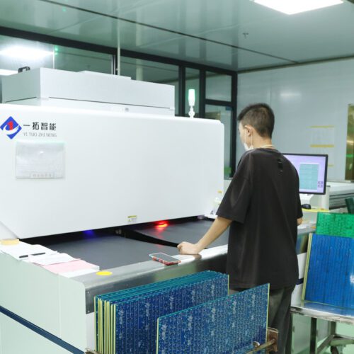
6-layer fabrication requires two inner layer imaging cycles (for the two inner signal layers and two plane layers) with registration targets verified by X-ray drill after lamination. Our lamination uses vacuum-assisted hydraulic presses with controlled ramp rates (2-3°C/minute) and peak temperatures of 185-190°C for standard FR-4 cure. Each inner layer pair undergoes AOI verification before lamination, creating a hold point that prevents defective innerlayers from proceeding to subsequent processing. Impedance coupons are included on each production panel, with TDR measurements reported at ±7% tolerance for single-ended lines and ±10% for differential pairs. Electrical testing detects opens and shorts on 100% of boards. For Class 3 builds, ionic contamination testing per IPC-TM-650 2.3.25 verifies cleanliness below 1.56μg NaCl/cm² equivalent.
Leave a message
Email info@xinanpcb.com
WhatsApp 86-13825400918
WeChat xinanpcb
Back to top

All Products

Contact Us

Leave a message